Further in 65816

I wrote some 6502 ASM tutorials a while back.

26. ASM Basics

Feel free to check them out (5 pages total). You can test various things with this online 6502 emulator…

https://skilldrick.github.io/easy6502/

All the information here will transfer perfectly toward 65816 programming. Stay on this until you understand it, before moving on to any more.

Or, if you prefer video tutorials…

Opcodes References 6502

http://www.6502.org/tutorials/6502opcodes.html

http://www.obelisk.me.uk/6502/reference.html

Quick Explanation of 65816 ASM

I will just cover some basics, and then mention the differences between 6502 and 65816.

Data transfer.

You need to load data to a register to move it. Any of the registers can do this.

LDA $1000 ; load A from address $1000
STA $800 ; store/copy A to address $800

LDX $1000 ; load X from address $1000
STX $800 ; store/copy X to address $800

LDY $1000 ; load Y from address $1000
STY $800 ; store/copy Y to address $800

and, depending on register size this would move 1 byte or 2. If it moved 2 bytes, it would get the lower byte from $1000 and the upper byte from $1001.

Note, you can write comments in ASM with a ; semicolon. Everything after the semicolon is ignored by the assembler.

Addressing modes.

Depending on how the LDA is written in assembly, you can perform multiple kinds of operations.

Direct Page

(similar to the zero page from 6502)

LDA $12 – load A from the direct page address $12. If direct page register is $0000 this will load A from $000012 (direct page is always in the $00 bank).

Absolute

LDA $1234 – loads A from the address $1234, in the bank defined by the Data Bank Register. If the Data Bank is $00… will load A from $001234.

Absolute Long

LDA $123456 – loads A from address $3456 in the $12 bank.

Immediate

LDA #$12 – loads A with the value $12. Always needs a preceding #. Might be an 8 bit or a 16 bit value depending on the mode of A.

Direct Page Indexed

Indexed modes are for arrays of bytes, using index registers to select an element of that byte array. Direct page is always in bank zero.

LDA $12, X – same as direct page, but the X register is added to the address number. If X is $10, this would load A from the address $22.

LDA $12, Y – same, but the Y register is added to the address number.

(X and Y are NOT restricted to 8 bit, and can extend $ffff bytes forward, except that the final address bank will be $00. Direct page mode always uses bank $00 as the final location.)

Absolute Indexed

LDA $1234, X – same as absolute, but the X register is added to the address number.

LDA $1234, Y – same as absolute, but the Y register is added to the address number.

(X and Y don’t wrap, and if address + X > $ffff it will temporarily increase the data bank byte to extend into the next bank. This is true of every indexed mode except for the direct page indexed.)

Absolute Indexed LongĀ 

LDA $123456, X – same as absolute long, but the X register is added to the address number. (only X can do this mode)

Indirect

This is how pointers work on the 6502 (65816) CPU. The pointer is loaded to 2 consecutive direct page addresses.

LDA ($12) – $12 is an address in the Direct Page. It takes a byte from $12 (lower byte) and $13 (upper byte) to construct an address, then the bank byte from data bank register, and then loads from that address. If $12 = $00 and $13 = $80, then this would load A with the value at address $018000 (if the data bank is $01).

Indirect Long

Like Indirect, but 3 consecutive bytes are stored in the Direct Page to construct a long address. Low byte, High byte, then Bank byte.

LDA [$12] – If $12 = $00 and $13 = $80 and $14 = $02, loads A from the value at address $028000.

Indirect, Y

LDA ($12), Y – same as Indirect, but the indirect address is added to the Y register to get a final address to load to A from.

Indirect Long, Y

LDA [$12], Y – same as Indirect Long, but the indirect long address is added to the Y register to get a final address to load to A from.

Indirect, X

This is for an array of pointers. Each pointer (2 bytes each) is in the Direct Page, and you will need to increase X by 2 to switch between them.

LDA ($12, X) – Let’s say X is 2, so we don’t want to look at RAM addresses $12 and $13, but rather $14 and $15. RAM address $14 holds the value 00, RAM address $15 holds $80, and the data bank is $01. This will load A with the value at address $018000.

.

https://wiki.superfamicom.org/65816-reference

Changes in the 65816 (from 6502)

** If you don’t understand all these things, don’t worry. You can always come back to it later, as these things come up. I frequently have to check the WDC manual to be reminded of all the details of each instruction, and I’ve been doing this 10 years. **

Zero page has been replaced with direct page, which is movable by changing the DP register. Just keep it $0000 for most purposes.

The hardware stack is no longer fixed. It can be any address in the zero bank. (on the SNES should be set at $1fff at the start of the program).

The A, X, and Y registers can be 8 or 16 bits. See SEP / REP below.

Many operations can now be 8 or 16 bytes depending on the size of the A register. ADC, AND, ASL, BIT, CMP, DEC, EOR, LDA, LSR, ORA, PHA, PLA, ROL, ROR, SBC, STA, STZ, TRB, and TSB… are all dependent on the size of the A register.

BRK has its own vector. Could be used for software purposes or debugging.

.

NEW INSTRUCTIONS

Long addressing

(can’t be Y)
ADC long
ADC long, X
AND long
AND long, X
CMP long
CMP long, X
EOR long
EOR long, X
JMP long aka JML
JSR long aka JSL (also RTL return long)
LDA long
LDA long, X
ORA long
ORA long, X
SBC long
SBC long, X
STA long
STA long, X

Store Zero

Stores zero at an address without changing A. (1 or 2 bytes depending on size of A)
STZ dp
STZ dp, X
STZ absolute
STZ absolute, X
(can’t do long)

Branching

BRA branch always
BRL branch always long (2 bytes, signed)
(don’t use BRL, just do JMP. BRL is for a system that might load a program anywhere in the RAM, relocatable code. Not really for the SNES.)

JMP (indirect) will look for a 2 byte address on bank zero, and jump to an that address, but always jumping to the current program bank. If it says JMP ($1234) it will look at $001234 and $001235. If 001234 is $50 and 001235 is $60, it will jump to address $6050 in the current program bank.

JMP [indirect long] will look for a 3 byte address on bank zero, and combine them to create a long jump address to anywhere. If the 2 byte value in brackets is [$1234] it will look at $001234, $001235, and $001236 for the 3 bytes, combine them to a long address, and jump to that.

JMP (indirect, X) is for an array of function pointers (a jump table), using X to switch between the different indirect jump addresses. Unlike JMP (indirect), which looks for the indirect address on the zero bank, the JMP (indirect, X) mode will look for the indirect address in the CURRENT PROGRAM BANK. (and it will jump to an address in the current program bank). X should be an even number. You should have a table of addresses (2 bytes each) at this location, and use X to choose which one. This indirect jump is the most useful. Remember it.

JSR (indirect, X) . same as above, except you can return from the function with RTS.

INC / DEC

now available for the A register.

dec A . is the same as A = A – 1
inc A . is the same as A = A + 1

Indirect with or without Y Index

(dp means that the pointer needs to be located in the direct page)
ADC (dp) . . ADC (dp), Y
AND (dp) . . AND (dp), Y
CMP (dp) . . CMP (dp), Y
EOR (dp) . . EOR (dp), Y
LDA (dp) . . LDA (dp), Y
ORA (dp) . . ORA (dp), Y
SBC (dp) . . SBC (dp), Y
STA (dp) . . STA (dp), Y

Indirect Long and Indirect Long Indexed

With or without Y indexing

ADC [dp] . . ADC [dp], Y
AND [dp] . . AND [dp], Y
CMP [dp] . . CMP [dp], Y
EOR [dp] . . EOR [dp], Y
LDA [dp] . . LDA [dp], Y
ORA [dp] . . ORA [dp], Y
STA [dp] . . STA [dp], Y
SBC [dp] . . SBC [dp], Y

SEP/REP

To set register size, we use REP or SEP (reset processor flag, set processor flag).
REP #$20 set A 16 bit
SEP #$20 set A 8 bit
REP #$10 set XY 16 bit
SEP #$10 set XY 8 bit
or combine them…
REP #$30 set AXY 16 bit
SEP #$30 set AXY 8 bit

(REP and SEP can be used to change other processor status flags).

(note the # for immediate addressing)

Transfers between registers.

now include
TXY – transfer x to y
TYX – transfer y to x
TCS – transfer A register to stack pointer
TSC – transfer stack pointer to A register

Size mismatch from transfers between A and index registers X or Y. Think about the destination size, that will tell you how many bytes will transfer.
A8 -> X16 or Y16 transfers 2 bytes, remember that A in 8 bit, the high bit exists
A16 -> X8 or Y8 transfers 1 byte
X8 or Y8 -> A16 transfers 2 bytes, and the upper byte of A is zeroed. XY in 8 bit always have zero as their upper byte.
X16 or Y16 -> A8 transfers 1 byte, the upper byte of A unchanged

Stack Relative

Uses the stack pointer as a base, added to a constant as the index.

You would push variables to the stack before calling a jsr or jsl.
The stack pointer is always points to 1 less than the last value pushed, so start from 1. If JSR to a function, then add 2 more. If JSL to a function then add 3 more.

ADC sr, S
AND sr, S
CMP sr, S
EOR sr, S
LDA sr, S
ORA sr, S
SBC sr, S
STA sr, S

Example… STA 1, S

Stack Relative Indirect

Push a pointer to an array to the stack. Index that array with Y.
ADC (sr, S), Y
AND (sr, S), Y
CMP (sr, S), Y
EOR (sr, S), Y
LDA (sr, S), Y
ORA (sr, S), Y
SBC (sr, S), Y
STA (sr, S), Y

Block Moves

To copy a chunk of bytes from one memory area to another. MVN Block Move Next and MVP Block Move Previous.

You are supposed to use MVN to move from a lower address to a higher one, and MVP from a higher address to a lower. For MVN, X holds the start address of src and Y holds the start address of dest, and A (always 16 bit, regardless of size of A) holds the # of bytes to transfer minus 1. For MVP, X holds the end address of the src block and Y holds the end address of the dest block.

Just use MVN, it’s easier to use.

The byte order in the binary is opposite of what the standard syntax indicates, so I tend to use a macro to handle this, because it’s confusing. And there was a change in ca65 source code which reverses the order, so code will break if you use the wrong version of ca65 (grumble).

MVN src bank, dest bank
MVP src bank, dest bank

The registers should be 16 bit before using MVN or MVP. Also, they have an annoying issue, where they will overwrite the data bank register, so it is probably a good idea to push that register to the stack before MVN/MVP and restore it (pull it from the stack) after the MVN/MVP procedure.

Push to stack

PEA address
PEI (dp)
PER relative-address

PEA which is called push effective “address”, but it really just pushes a 16 bit value to the stack without using a register. It doesn’t have to be an address. It is very useful for any 16 bit immediate push to the stack. You don’t need to change a register size either, it always pushes a 16 bit value.

PEI pushes a (16 bit) value stored on the direct page (in bank zero) to the stack.

PER pushes a value from the same bank, in a 16 bit relative distance from this instruction. You could use stack relative or pull it to a register from after pushing the value or address to the stack.

NOTE: the standard syntax here is confusing for PEA and PEI. PEA actually works like a 16-bit immediate mode, but (for unknown reasons) omits the # hash. PEI actually works like Direct Page Addressing, but (for unknown reasons) has unnecessary parentheses () making it look like an Indirect Mode. I have reread the documents 4-5 times and it works like PEI $12… but the official syntax is PEI ($12). ca65 expects the official syntax.

Pushing / pulling the new registers

PHB – push data bank register to stack
PHD – push direct page register to stack
PHK – push program bank register to stack
PHX – push X register to stack
PHY – push Y register to stack
PLB – pull from stack to data bank register
PLD – pull from stack to direct page register
PLX – pull from stack to X register
PLY – pull from stack to Y register

Transfers with A

(always copies 16 bits regardless of size of A)
TCD – transfer from A to direct page register
TCS – transfer from A to stack pointer
TDC – transfer from direct page register to A
TSC – transfer from stack pointer to A

Test and Set Bits / Test and Reset Bits

TRB dp
TRB address
TSB dp
TSB address

TRB, test and reset bits. A register (8 or 16 bits) has the bits to change. If a bit in A is 1 it will be zeroed at the address location. If a bit in A is 0 it remains unchanged.

TSB, test and set bits. A register (8 or 16 bits) has the bits to change. If a bit in A is 1 it will be set (1) at the address location. If a bit in A is 0 it remains unchanged.

There is also a testing operation, as if the value in A was ANDed with the address, and the z flag is set if A AND value at address would equal zero. Unrelated to the setting or resetting operation.

More

COP – jump to COP vector (for a coprocessor routine)
XBA – swap high and low bytes of A (works even if A is 8 bit)
XCE – move carry to CPU mode (emulator or native modes)
STP – stops the CPU, only reset will start it again. Don’t use this.
WAI – wait till interrupt, halts the CPU until IRQ or NMI trigger.
WDM # – nothing, but useful for debugging. Followed by a number, which could be used to locate where you are in the code (in a debugger).

(in older version of ca65, WDM won’t work. I think it was fixed around 2017.)

Some more links, to other descriptions of 65816 ASM

https://www.smwcentral.net/?p=section&a=details&id=14268

http://6502.org/tutorials/65c816opcodes.html

And these links again, for reference.

https://wiki.superfamicom.org/65816-reference

Programming the 65816

SNES main page

.

65816 Basics

Programming the SNES in assembly, using the ca65 assembler.

Assembly Language Basics

Assembly is a low level programming language. We have to think at the basic level that the CPU processes the binary code. Let’s review binary, and hexadecimal numbers.

Number Systems

Binary. Under the hood, all computers process binary numbers. A series of 1s and 0s. In the binary system, each column is 2x the value of the number to the right.

0001 = 1
0010 = 2
0100 = 4
1000 = 8

You then add all the 1’s up

0011 = 2+1 = 3
0101 = 4+1 = 5
0111 = 4+2+1 = 7
1111 = 8+4+2+1 = 15

Each of these digits is called a bit. Typically, there are 8 bits in a byte. So you can have numbers from
0000 0000 = 0
to
1111 1111 = 255

Since it is difficult to read binary, we will use hexadecimal instead. Hexadecimal is a base 16 numbering system. Every digit is 16x the number to the right. We use the normal numbers from 0-9 and then letters A-F for the values 10,11,12,13,14,15. In many assembly languages, we use $ to indicate hex numbers.

$0 = 0
$1 = 1
$2 = 2
$3 = 3
$4 = 4
$5 = 5
$6 = 6
$7 = 7
$8 = 8
$9 = 9
$A = 10
$B = 11
$C = 12
$D = 13
$E = 14
$F = 15

$F is the same as binary 1111.

The next column of numbers is multiples of 16.

$00 = 16*0 = 0 _____ $80 = 16*8 = 128
$10 = 16*1 = 16 _____ $90 = 16*9 = 144
$20 = 16*2 = 32 ____ $A0 = 16*10 = 160
$30 = 16*3 = 48 ____ $B0 = 16*11 = 176
$40 = 16*4 = 64 ____ $C0 = 16*12 = 192
$50 = 16*5 = 80 ____ $D0 = 16*13 = 208
$60 = 16*6 = 96 ____ $E0 = 16*14 = 224
$70 = 16*7 = 112 ____ $F0 = 16*15 = 240

$F0 is the same as binary 1111 0000.
add that to $0F (0000 1111) to get
$FF = 1111 1111

So you see, you can represent 8 bit binary numbers with 2 hex digits. From $00 to $FF (0 – 255).

To get the assembler to output the value 100 you could write…

.byte 100

or

.byte $64

.

16 bit numbers

Typically (on retro systems) you use 16 bit numbers for memory addresses. Memory addresses are locations where pieces of information can be stored and read later. So, you could write a byte of data to address $1000, and later read from $1000 to get that data.

The registers on the SNES can be set to either 8 bit or 16 bit modes. 16 bit mode means it can move information 16 bits at a time, and process the information 16 bits at a time. 16 bit registers means that it will read a byte from an address, and another from the address+1. Same with writing 16 bits. It will write (low order byte) to the address and (high order byte) to address+1.

In binary, a 16 bit value can go from
0000 0000 0000 0000 = 0
to
1111 1111 1111 1111 = 65535

In hex values, that’s $0000 to $FFFF.

Let’s say we have the value $1234. The 12 is the most significant byte (MSB), and the 34 is the least significant byte (LSB). To calculate it’s value by hand we can multiply each column by multiples of 16.

$1234
4 x 1 = 4
3 x 16 = 48
2 x 256 = 512
1 x 4096 = 4096
4096 + 512 + 48 + 4 = 4660

To output a 16 bit value $ABCD, you could write

.word $ABCD
(outputs $cd then $ab, little endian style)

Don’t forget the $.

We can also get the upper byte or lower byte of a 16 bit value using the < and > symbols before the value.

Let’s say label List2 is at address $1234

.byte >List2
will output a $12 (the MSB)

.byte <List2
will output a $34 (the LSB).

.

24 bit numbers

We can now access addresses beyond $ffff. There is a byte above that called the “bank byte”. Using long 24 bit addressing modes or changing the data bank register, we can access values in that bank using regular 16 bit addressing. Here is an example of a 24 bit operation.

LDA f:$7F0000
will read a byte from address $0000 of the $7F bank (part of the WRAM).

In ca65, the f: is to force 24 bit values from the symbol / label. The assembler will calculate the correct values. (to force 16 bit you use a: and to force 8 bit you use z:)

JML $018000
will jump to address $8000 in bank $01.

To output a 24 bit value
.faraddr $123456
(outputs $56…$34…$12)

Or you could do this, to output a byte at a time.
.byte ^$123456
(outputs $12)
.byte >$123456
(outputs $34)
.byte <$123456
(outputs $56)

But we don’t want to write our program entirely using byte statements. That would be crazy. We will use assembly language, and the assembler will convert our three letter mnemonics into bytes for us.

LDA #$12
(load the A register with the value $12)

will be converted by the assembler into this machine code that the 65816 CPU can execute…

$A9 $12

.

65816 CPU Details

There are 3 registers to work with

A (the accumulator) for most calculations and purposes

X and Y (index registers) for accessing arrays and counting loops.

A,X, and Y can be set to either 8 bit or 16 bit. The accumulator is sometimes called C when it is in 16 bit mode. Setting the Accumulator to 8 bit does not destroy the upper byte, you can access it with XBA (swap high and low bytes). However, setting the Index registers to 8 bit will delete the upper bytes of X and Y.

There is a 16-bit stack pointer (SP or S) for the hardware stack. If you call a function (subroutine) it will store the return address on the stack, and when the function ends, it will pop the return address back to continue the main program. The stack always exists on bank zero (00). The stack grows downward, as things are added to it.

Processor Status Flags (P), are used to determine if a value is negative, zero, greater/lesser/equal to, etc. Used to control the flow of the program, like if/then statements. Also the register size (8 bit or 16 bit) are set/reset as status flags. *(see below)

There is a 16-bit direct page (DP) register, which is like the zero page on the 6502 system, except that it is now movable. Typically, people leave it set to $0000 so that it works the same as the 6502. Zero page is a way to reduce ROM size, by only using 1 byte to refer to an address. The DP always exists on bank zero (00).

The Program Bank Register (PBR or K) is the bank byte (highest byte) of the 24 bit address of where the program is running. Together, with the program counter (PC) the CPU will execute the program at this location. The PBR does NOT increment when the PC overflows from FFFF to 0000, so you can’t have code that flows from one bank to another. You can’t directly set the PBR, but jumping long will change it, and you can push it to the stack to be used by the…

Data Bank Register (DBR or B) is the bank byte (highest byte) of the 24 bit address of where absolute addressing (16 bit) reads and writes. Usually you want to set it to the same as where your program is running. You do it with this…

PHK (push program bank to stack)
PLB (pull from stack to data bank)

But you can also set it to another bank, to use absolute addressing to access that bank’s addresses.

There is also a hidden switch to change the processor from Native Mode (all 65816 functions) to Emulation Mode (compatibility for legacy 6502 software, with direct page fixed to $0000-00ff, stack fixed to $0100-01ff, registers fixed to 8 bit only). The CPU powers on in Emulation Mode, so you will usually see

CLC (clear the carry flag)
XCE (transfer carry flag to CPU mode)

near the start, to put it in Native Mode. That’s what we want, native mode.

.

Status Flags

NVMXDIZC
– – – B – – – – (emulation mode only)

N negative flag, set if an operation sets the highest bit of a register
V overflow flag, for signed math operations
M Accumulator size, set for 8-bit, zero for 16-bit
X Index register size, set for 8-bit, zero for 16-bit
D decimal flag, for decimal (instead of hexadecimal) math
I IRQ disable flag, set to block IRQ interrupts
Z zero flag, set if an operation resets a register to zero
. . . . or if a comparison is equal
C carry flag, for addition/subtraction overflow

B break flag, if software break BRK used.

.

Where does the program start? It always boots in bank zero, in emulation mode, and pulls an address (vector) off the Emulation Mode Reset Vector located at $00FFFC and $00FFFD, then jumps to that address (always jumping to bank zero). Your program should set it to Native Mode, after which these are the important vectors.

IRQ $00FFEE-00FFEF (interrupt vector)
NMI $00FFEA-00FFEB (non-maskable interrupt vector)

If an interrupt happens, it will jump to the address located here (always jumping to bank zero).

There is no Reset Vector in Native Mode. Hitting reset will automatically put it back into Emulation Mode, and it will use that Reset Vector.

But more on those later.

I highly recommend you learn more about 6502 assembly before continuing. Here are some links that are helpful.

http://www.6502.org/tutorials/6502opcodes.html

https://skilldrick.github.io/easy6502/

https://archive.org/details/6502_Assembly_Language_Programming_by_Lance_Leventhal/mode/1up

and 65816 assembly reference here.

https://wiki.superfamicom.org/65816-reference

and for the very bold, the really really big detailed book on the subject. You might want to download it just for reference.

Programming the 65816

SNES main page

SNES Overview

SNESconsole

The Super Nintendo first came out in 1991 (1990 in Japan as the Super Famicom). It was one of the best game consoles of all time, with an amazing library of games. It definitely has a special place in my heart. Before we get to programming for it, let’s take a look and see what’s under the hood.

It contains a 65816 clone chip called the Ricoh 5A22 (3.58 MHz), which is a direct descendant of the 6502 chip that powers the original Nintendo. The instruction set is a super-set of the 6502 instruction set, and essentially all the 6502 codes work the same on both chips (with the bugs fixed). The chip has both 8 bit and 16 bit modes, and has a full 24 bit addressing space (0 to 0xFFFFFF).

(borrowed this image from https://copetti.org/projects/consoles/super-nintendo/ )

motherboard_marked

It has 128kB internal WRAM.

This unit has 2 PPU chips. Later models had 1 chip (marked as “1chip”) and are slightly better, but both function the same, other than picture quality. The PPU is what generates the video image. It has its own 64 kB of VRAM (arranged as 32 kB addresses of 16 bits). The VRAM holds our graphics and background maps.

Background tiles can be 8×8 or 16×16. Background maps can be 32×32, 64×32, 32×64, or 64×64 tiles in size (multiplied by the tile size). Giving from 256×256 pixel map (8×8 tiles and 32×32 map) to 1024×1024 pixel map (16×16 tiles and 64×64 map). Scrolling games will typically change the map as you move through the level… to give the appearance of an even larger map.

There is also a memory chip for color palettes (CGRAM) of 512 bytes. Color palettes are 15 bits per color, RBG 0bbbbbgggggrrrrr, so 512 bytes gives us a total of 256 colors. AndĀ  another RAM chip for sprite attributes (OAM) of 544 bytes, arranged as a low table of 512 and a high table of 32.

Sprites are 4 bytes (and 2 extra bits) each, so 512 byte / 4 gives us 128 sprites displayable at once. Sprites can be various sizes, from 8×8 to 64×64. Typically they would be 8×8 or 16×16.

The CIC is the security chip. Each cartridge will need a matching chip to run.

The cartridge itself could contain battery backed SRAM for saving games. The cartridge can also have co-processors, such as the SuperFx chip.

On the other side of the motherboard are the audio chips. The audio CPU is marked S-SMP. It is a system that runs independently from the SNES CPU. This processor is a Sony SPC700 Audio CPU. It has it’s own 64 kB of RAM where you load the audio program, the song data, and the audio samples.

The audio program will then process the song data and set the 8 channels (DSP, digital signal processor) to play the different audio samples at different rates to generate different tones. The samples are compressed in a format called BRR.

When the SNES is switched on, the main program will have to load everything to the audio ram. This is actually a very slow process, and if you notice that games show a black screen for a few seconds when the game is first run, it is probably due to loading the sound RAM. Once the audio program is loaded, it will run automatically. The audio program can also get signals from the game (for example, to change songs, or to play a sound effect).

Graphics Modes

If you are familiar with the original Nintendo, the Super Nintendo works very similar except that everything is changeable. Backgrounds can have 8×8 or 16×16 tiles, small maps, large maps, 1 layer, 2 layers, 3 layers, 4 layers, all moving independently.

You can rearrange the VRAM any way you want. You can put maps first then BG tiles then sprite tiles. Or, BG tiles first then sprite tiles then BG maps. Or, you can have one giant 256 color BG that fills the entire VRAM and no sprite tiles. Any way you want.

Here’s a quick look at the different background modes.

Mode 0

4 layers of 4 colors per tile.

This mode is not as colorful (per tile). I generally only see it used for screens of text. The main advantages are the extra layer, and the graphics files are half the usual size. This mode is the most like the original Nintendo (or maybe Gameboy Color), and a game ported from there to the Super Nintendo (with no improvements) might use mode 0.

(It’s actually 3 colors plus 1 transparent per tile. Each layer has a unique 8 palettes to choose from. 8 palettes x 3 colors x 4 layers + 1 backdrop color = 97 BG colors for Mode 0)

Mode 1

2 layers of 16 colors per tile.

1 layer of 4 colors per tile.

This is the most used mode. Nearly every game uses mode 1 most of the time. Typically, the first 16 color layer for foreground and other for background. Then the 4 color layer is used for text boxes or HUD / score display.

(8 palettes, both 16 color layers share the same 8 palettes. 15 colors per palette x 8 palettes + 1 backdrop color = 121 BG colors. The 4 color layer has to share palette space with the first palette of the other layers.)

SMW

Mode 2

2 layers of 16 color.

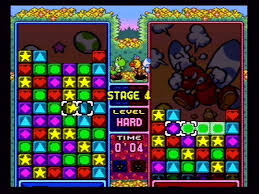
Each tile can be shifted. See Tetris Attack, how the play area scrolls upward. This mode is very rarely used. Yoshi’s Island uses it for 1 level (Touch Fuzzy Get Dizzy).

TetrisAttack

Mode 3

1 layer of 256 colors per tile.

1 layer of 16 colors per tile.

This mode is very colorful, but the graphics files are twice as big as usual, so games typically only used them (if at all) for title screens. Like this…

Aero the Acro-Bat (USA)_000

Mode 4

1 layer of 256 colors per tile.

1 layer of 4 colors per tile.

Similar to mode 2, tiles can be shifted. Rarely used mode. Bust-A-Move uses Mode 4 for regular gameplay.

Mode 5

1 layer of 16 colors

1 layer of 4 colors

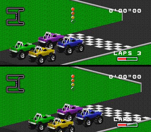
This mode is a high resolution mode. It is rarely used. RPM Racing uses it.

rpm-racing-usa_000

Mode 6

1 layer of 16 color

Also a high resolution mode. Also can shift tiles like mode 2 or 4. I’ve never seen this used outside of demos.

Mode 7

1 layer of 256 colors

This is the mode that really set Super Nintendo apart from other consoles. This mode is one layer that can zoom in and out and rotate the background. This mode is completely different from the other modes and has it’s own special graphics format that is hard to explain. Tiles are always 8×8 pixel and the map is always 128×128 tiles, giving a 1024×1024 pixel map.

Fzero

Interestingly, mode 7 does not naturally do perspective. It can stretch and rotate only. But, games like F-zero change the stretching parameters line by line to simulate perspective. As the PPU generates the image sent to the TV, it renders each horizontal line, one at a time, and the BG image becomes more and more zoomed in towards the bottom of the screen.

Really, all the modes can change parameters line by line. One fairly common technique is to change the main background color to create a gradient effect. It uses HDMA to do this, which is the only way to send data to the VRAM (or in this case, CGRAM) during the active screen time.

Batman

Sprites

For all the modes, the way sprites work is always the same. Sprites are always 16 colors (actually 15 since the 0th color always transparent). Also, sprites have different size modes (8×8, 16×16, 32×32, 64×64), and different priorities (which work like layers). You can flip them horizontally or vertically.

Like the NES, there is a limit of how many sprites can be displayed on each horizontal line, and the calculus for that is a bit complicated. If you split each large sprite into 8×1 slices, you can only fit 32 slices on a horizontal line. The 33rd will be invisible. Generally this isn’t a problem, but you should be aware of it.

All the characters on the screen are sprites. Mario. Koopas. Etc. Because sprites can be large and you can fill the screen with them, and move them around easily, sprites can be used for background elements and be considered as another background layer. Title screens often have the title written in sprites, for example. And, mode 7 games use sprites as a second layer.

Other possibilities

You can change modes and settings mid screen.

You can change scrolling mid screen, and create a shifting sine wave pattern, perhaps for fire or underwater scene.

You can do color transparencies. One layer added to another (or subtracted from another).

You can use “windows” to cut a hole in the screen, or narrow the screen from the sides, or even adjust the windows line by line with HDMA and draw shapes on the screen.

All these effects are more advanced, and we shouldn’t worry too much about that stuff yet.

I plan to write some basic tutorials for getting a very simple game working on the Super Nintendo. But, we need to take it very slowly.

SNES main page