SNES programming tutorial. Example 6.
https://github.com/nesdoug/SNES_06
.
Warning – this was made with SPEZ, version 2. Version 3’s default metasprite data breaks the code used in the example because it has 2 extra bytes for flipping the metasprite horizontally and/or vertically. If you use version 3 with the code below, you need to uncheck ‘flip data’. Or, you could use the metasprite code provided with SPEZ v3 in the ‘example’ folder. Or, a third option, you can still download version 2 of SPEZ.
https://github.com/nesdoug/SPEZ
.
Controller reads
There is a set of registers that can be read like NES registers. Originally, they wanted to make it easy to transition from programming NES games to programming SNES games. They even used the same number $4016 and $4017 (ports 1 and 2). However, you shouldn’t read these. Instead you should turn on the auto-read feature (and also the NMI enable) from register $4200.
With auto-controller reads set, the CPU be interrupted (soon after the end of each frame) and automatically read all the buttons from both controllers and then store the values at $4218-$421b.
$4218-19 port 1
$421a-1b port 2
(if a multitap for 4 player games installed, 421c-d and 421e-f for controllers 3+4)
The button order is…
KEY_B = $8000
KEY_Y = $4000
KEY_SELECT = $2000
KEY_START = $1000
KEY_UP = $0800
KEY_DOWN = $0400
KEY_LEFT = $0200
KEY_RIGHT = $0100
KEY_A = $0080
KEY_X = $0040
KEY_L = $0020
KEY_R = $0010
And I use these constants as a bit mask (bitwise AND operation) to isolate the buttons.
The pad_poll function also does some bit twiddling to figure out which buttons have just been pressed this frame.
pad1 and pad2 variables tell you which buttons are being pressed.
pad1_new and pad2_new tell you which buttons have just been newly pressed this frame.
We need call pad_poll each frame. How do we know that a new frame has started? That’s where the NMI comes in.
NMI
When the screen is on, the PPU spends most of its time drawing pixels to the screen, one horizontal line at a time, one pixel at a time. Starting at the top, it goes left to right and draw a line. Then it jumps down and draws the next line. Etc, etc, until the frame is completed.
While it is drawing pixels to the screen, the PPU is busy, you can’t send new data to the VRAM. You can’t send new data to the OAM or the CGRAM (palette) either. After the screen is done drawing, the PPU rests in a vertical blank period for a little bit. During this v-blank period, you CAN access the PPU registers.
If you turn on NMI interrupts, when the PPU is done drawing to the screen… nearly at the very beginning of v-blank, the PPU sends an NMI signal to the CPU. This happens every frame, which is 60 times a second (50 in Europe). That signal causes the CPU to pause and jump to the NMI vector (an address it finds at $00ffea in the ROM). We have it set to jump to the label called NMI: which is located in the init.asm file. (note, the NMI code needs to be in the 00 bank).
The NMI code is just this.
bit $4210 *
inc in_nmi
rti
* ; it is required to read this register during NMI
(many game have much more elaborate NMI code than this)
Our main code is waiting for the in_nmi variable to change. When it changes we know that we are in the v-blank period. Now is a good time to write to PPU registers or send data to the VRAM. But, also, we are using this to time our game loop.
wait_nmi: waits until we are in v-blank. We call this at the top of the game loop. Notice that I put a WAI (wait for interrupt) instruction here. If you neglected to turn NMI interrupts on, this would crash the game, as it waits forever for a signal that never comes. IRQ interrupts could also trip the WAI instruction, which is why I also wait for the in_nmi variable to change to be sure. You could delete the WAI instruction, if you would like*. Some games use this waiting loop to spin a random number generator. You could do that as well…. like adding a large prime number over and over, or just ticking a variable +1 over and over.
* someone told me that WAI could make an emulator run less laggy, as it would have less to do each frame. It also saves electricity, because the CPU uses less while it waits. You decide if you need it or not.
Soon after the wait_nmi function runs, we run our DMA to the OAM (copy our sprite buffer to the sprite RAM). This needs to be done during v-blank, which is why we do it first. Then, we run our pad_poll to read new button presses. Then we enter the game logic. Here’s an example of what we are doing to move the sprite.
Our sprite is composed of 3 sprites that move together (16×16 each). Each time we press the right button, we need to increase the X value of each sprite. Left, we decrease the X values. Each sprite uses 4 bytes, so each sprite X value is 4 bytes apart. So we do this…
  AXY16
  lda pad1
  and #KEY_LEFT
  beq @not_left
@left:
  A8
  dec OAM_BUFFER ;decrease the X values
  dec OAM_BUFFER+4
  dec OAM_BUFFER+8
  A16
@not_left:
LDA loads the A register with pad1, which has all the button presses for controller 1. We apply a bit mask (AND) to isolate the left button. If it is zero, the button isn’t being pressed, and it will branch (BEQ) over our code. Otherwise, it will then to the dec OAM_BUFFER lines. Dec can be 8 bit or 16 bit, depending on the size of the A register. We want 8 bit, so we A8 for that. We need the A16, to make sure we exit this bit of code with A always in 16 bit mode.
We repeat that process 3 more times for RIGHT, UP, and DOWN buttons. You see, our character moves around the screen. This code isn’t very good, though. We aren’t handling that 9th X bit.
With this code, you can move smoothly off the top and bottom of the screen, like this…

But if you try to move left off screen, it suddenly disappears. Like this below…

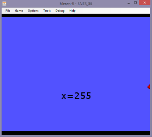
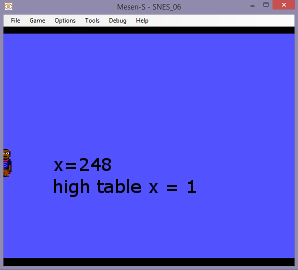
That’s why we need that 9th X bit in the high table. Here’s what it looks like at X=248, with the 9th bit = 0.

And below shows what the same X=248, with the high table (9th bit) = 1
We didn’t do that in this example, but I worked up some code that can manage this. If you look in the next example files, in the library.asm file, you will see the functions called OAM_Spr and OAM_Meta_Spr. The spr_x variable is 9 bit so that we can move a sprite object smoothly off the left side without suddenly disappearing.
https://github.com/nesdoug/SNES_07/blob/master/library.asm
To use OAM_Spr, first we set the variables spr_x, spr_y, spr_c (tile), spr_a (attributes), and spr_sz (size), then call this function, and it will load the OAM buffers with the appropriate values (and also handle that awkward high table).
To use OAM_Meta_Spr, we first set spr_x, and spr_y, and then load the A and X registers with the address of the metasprite data. (A16 with absolute address, and X with the bank #). The metasprite data is generated by SPEZ and it is a list of each sprite in the multi-sprite object (5 bytes per sprite). This function will automatically calculate the relative position of each sprite, and write them in the OAM buffers.
.


 layer 1
 layer 2
 layer 3